
- PV-Station-Solutions
- PV-Panel-Testing-Solutions
- Silicon-Ingot-Testing-Solutions
At the starting point of photovoltaic manufacturing, wafer quality directly determines cell efficiency and production yield. Vision Potential’s Raw Wafer PL Inspection System SC-SPL, based on the photoluminescence (PL) principle of silicon materials, accurately identifies defects in early-stage processes such as silicon ingots, raw wafers, and textured wafers without electrical contact, enabling true source quality control and cost savings.
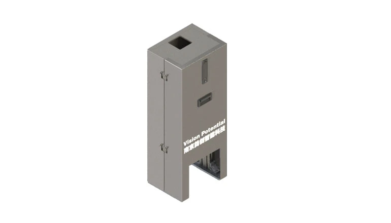
Vision Potential SC-SPL
Vision Potential’s silicon wafer PL inspection technology leverages the intrinsic excitation and luminescence characteristics of silicon—the fluorescence intensity emitted when excited electrons recombine is negatively correlated with defect density and recombination center concentration. This principle ensures that inspection results truly reflect the intrinsic quality of the silicon material, unaffected by electrical contact conditions.
From ingot grading and wafer sorting to texturing, diffusion, and other early battery manufacturing stages, the SC-SPL system delivers efficient intervention:
Wafer Production Quality Control: Integrated into sorters or texturing loaders for inline/offline inspection, ensuring incoming wafers meet standards.
Ingot Quality Analysis and Grading: Analyzes approximately 3mm-thick wafers cut from monocrystalline ingots, detecting black edges, black cores, and microcracks step by step to effectively remove defective material.
Pre-Texturing and Pre-Diffusion Inspection: High sensitivity enables detection of potential defects in low-lifetime process wafers, preventing subsequent resource waste.
University and Laboratory Research: Serves as a core tool for material intrinsic analysis and process optimization.
The system is equipped with a high-performance silicon wafer PL module, compatible with monocrystalline, quasi-monocrystalline, and polycrystalline wafers. It detects crystalline defects such as dislocations, wire marks, grain boundaries, blackening, concentric circles, and black corners—defects that are often missed by conventional appearance or microcrack modules. The system automatically calculates PL values based on grayscale and defect ratio, enabling quantitative defect severity grading, and supports integration with automated production lines for sorting signal output.
High Sensitivity: Suitable for low-lifetime wafers such as textured and diffused wafers, identifying issues at early stages.
Broad Compatibility: Supports 156–210mm half-cell and full-cell wafers, adapting to mainstream sizes.
Multi-Dimensional Data Analysis: Provides parameters such as black edge/black core index, non-uniformity index, and concentric circle index to aid process improvement.
Stable and Reliable: Features an NIR-enhanced InGaAs camera, 980nm semiconductor laser source, and industrial control platform, ensuring inspection accuracy and efficiency.
Vision Potential’s raw wafer PL inspection system has demonstrated its core value in production lines: by identifying defects early, it reduces the flow of defective wafers into downstream processes, significantly lowers manufacturing costs, and improves final cell performance consistency. Whether for photovoltaic manufacturers or material research institutions, the SC-SPL system is an ideal choice for quality control and process optimization.
contact
Be the first to know about our new product launches, latest blog posts and more. Nanjing Vision Potential Intelligent Technology Co.,Ltd.Established based on the Nanjing Xiangning Artificial Intelligence Research Institute, we have brought together a number of outstanding industry... Any question or request?
Click below, we’ll be happy to assist. contact