
- PV-Station-Solutions
- PV-Panel-Testing-Solutions
- Silicon-Ingot-Testing-Solutions

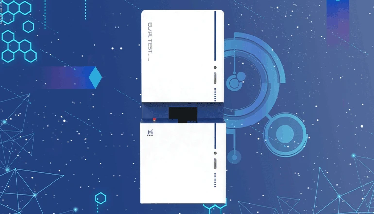
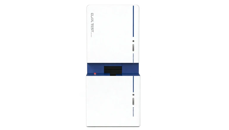
Crystalline Silicon/Perovskite PLEL All-in-One System is an innovative inspection device independently developed by Vision Potential. It integrates EL and PL dual-mode luminescence imaging capabilities, enabling synchronous benchmarking analysis of the same detection area and fully presenting the morphology and distribution of various defects. The device is equipped with a highly stable semiconductor laser light source (main wavelength 808±5nm, optional multi-band), paired with a high-sensitivity NIR camera, achieving high-resolution imaging of ≥0.1mm/pixel.
Covers crystalline silicon cells (PERC/TOPCon/HJT/xBC), single-junction perovskite cells, and tandem cells, supporting raw material control, process monitoring, finished product grading, and R&D innovation, providing quantitative data support for photovoltaic technology iteration.
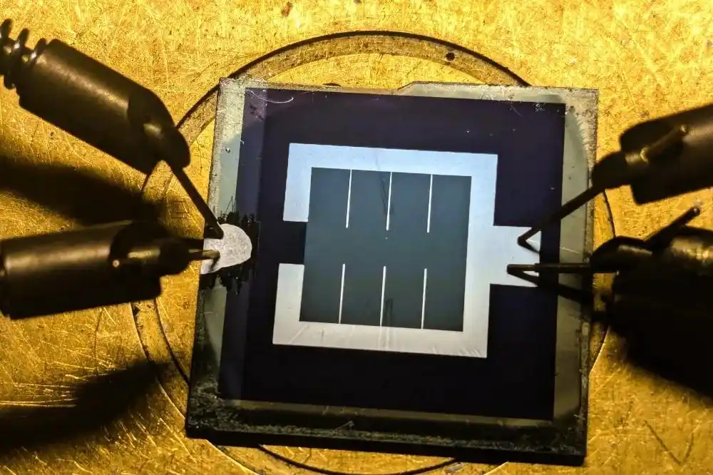
 SC-PLEL-PS Device Diagram
Analyze crystal structure and impurity distribution via PL, eliminate defects at the source, and reduce rework costs.
Capture defects caused by process fluctuations, provide quantitative data to support parameter adjustments, and ensure stable product quality.
Comprehensively inspect defects and evaluate performance, achieve product grading, ensure compliance with industry standards, and avoid downstream application risks.
Provide quantitative data for high-efficiency cell technology iteration and defect mechanism research, accelerating new technology industrialization.
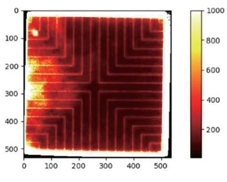
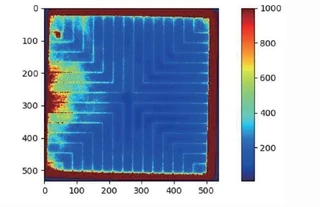
EL locks onto current blocking areas caused by cracks; PL identifies non-radiative recombination centers at grain boundaries, fully presenting defect morphology and distribution.
Intelligent control of cylinders/motors for automatic transport, position calibration, and lifting, significantly enhancing inspection efficiency and result repeatability.
808±5nm standard, optional 450/915/980nm; spot uniformity ≥90%, power adjustable 0.1~2 suns, precisely matching various cell excitation requirements.
NIR-enhanced camera, max frame rate 4.5FPS, imaging accuracy ≥0.1mm/pixel, capturing subtle defects.
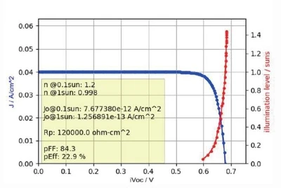
Proprietary algorithms analyze minority carrier diffusion length, lifetime (accuracy ±0.1μs, τ≤10μs), outputting IVoc, Jo, τ, Rs Mapping.
Constant current/voltage dual modes, voltage 0~30V (±1%), current 0~10A (±1%), precisely meeting different cell bias requirements.
Inspection Efficiency: ≤15 seconds per piece, suitable for full-process quality control in industrial mass production, quickly screening unqualified products and reducing subsequent packaging costs.
· Image Processing: Multiple adjustment methods and format saving
· Data Management: Automatic report generation and traceability
· Precise Observation: Cursor tracking and local statistics
· Intelligent Analysis: Automatic defect classification, MES interface
· Generate Mapping Graphs: IVoc, Jo, τ, Rs, etc.
· From Qualitative to Quantitative: Intuitive performance distribution display
· Suns-Voc Analysis, recombination study
| Parameter | Specification |
|---|---|
| Model | SC-PLEL-PS |
| Camera Specifications | NIR enhanced, 25MP, exposure 10μs~30s, response 400-1200nm |
| Infrared Pixels | 500~2500万像素 |
| Lens Specifications | HD wide-angle 8/16/25mm optional, FOV ≥80° |
| Light Source Specifications | Semiconductor laser, main wavelength 808±5nm (optional 450/915/980nm) |
| Spot Uniformity | ≥90% (within effective detection area) |
| Detection Cycle | 12μs~10000ms, step 1ms adjustable |
| Detection Wavelength Range | 900~1300nm (Crystalline Si), 700~900nm (Perovskite) |
| Detectable Defect Types | Cracks, broken grid, fragments, scratches, cold solder, over-etching, black spots, concentric circles, low-efficiency cells, contamination, etc. |
| Probe Configuration | 2~6 sets of pins, adjustable pitch, pure copper gold-plated (customizable) |
| Stage Size | 50×50mm ~ 230×230mm (larger customizable) |
| Control Method | Proprietary software fully automated control |
| Detection Accuracy | Crack width > 50μm detectable |
| Imaging Accuracy | ≥0.1mm/pixel |
| Focus Mode / Distance | Manual focus / 130-650mm |
| Hardware Mount | Aluminum profile, sheet metal, etc. |
| Inspection Time | 0.1s~10s (automatic based on object) |
| Test Platform | Windows platform |
| Constant Current/Voltage | 0~10A adjustable, accuracy ±1% / 0~30V adjustable, accuracy ±1% |
| Power | 1000-2000W |
| Power Supply Protection | Reverse current, overload, leakage, ESD, overheat protection |
| Computing Device | Industrial computer |
| Inspection Objects | Crystalline Si cells, single-junction Perovskite cells, Crystalline Si-Perovskite tandem cells (bare, with film, packaged) |
| Ambient Temperature | 15-50℃, Humidity 30%-70% (non-condensing) |
| Equipment Weight | Approx. 200kg (actual product prevails) |
| Dimensions | 1000×900×1600mm (L×W×H, actual product prevails) |
| Power Supply | Single-phase AC220V±10%, 50HZ±1HZ |
| Inspection Type | Inspection Object | B&W Imaging | False Color Imaging | Imaging Analysis |
|---|---|---|---|---|
| PL (Photoluminescence) | Crystalline Silicon Cell |  |  | Evaluate crystal quality and carrier lifetime via PL signal intensity: bright areas indicate good crystallization and long lifetime, dark lines/areas indicate cracks, metal impurities, etc. |
| Perovskite Cell | 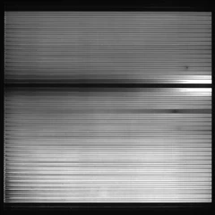 | 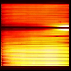 | Analyze film uniformity and defect state density: dark spots correspond to defect-rich areas or interface recombination centers. | |
| Perovskite Tandem - Perovskite Layer | 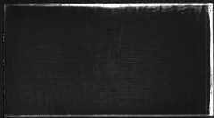 | 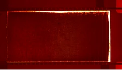 | Focus on intrinsic properties and interface matching of the perovskite layer; abnormal luminescence decay indicates high interface state density. | |
| Perovskite Tandem - Crystalline Si Layer | 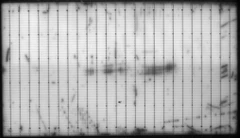 | 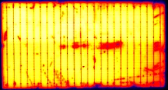 | Targeted detection of cracks, contamination in the crystalline Si layer, quantify carrier lifetime, assess tandem structure impact. | |
| EL (Electroluminescence) | Crystalline Silicon Cell | 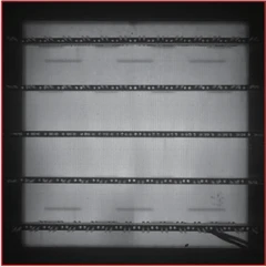 | 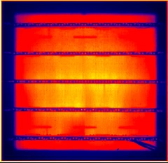 | Identify electrode contact abnormalities and carrier transport; dark areas may indicate cracks or broken grid. |
| Perovskite Cell |  | 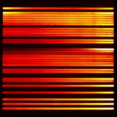 | Identify defect types and current distribution uniformity; dark spots indicate scribing deviations, cracks, or bad cells. | |
| Perovskite Tandem - Perovskite Layer | 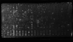 | 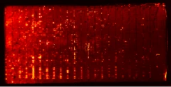 | Evaluate interlayer compatibility and current matching; abnormal luminescence indicates carrier injection/extraction obstacles. | |
| Perovskite Tandem - Crystalline Si Layer | 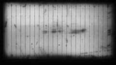 |  | Analyze crystalline Si layer electrode contact and overall synergy, avoid local current crowding leading to efficiency loss. |
Detects minority carrier diffusion length, minority carrier lifetime (accuracy ±0.1μs), micro-cracks/broken grid/black spots/concentric circles and other defects.
Supports IVoc, Jo, τ, Rs Mapping quantitative analysis, automatic report generation and traceability.
Gold-plated probe design, 2~6 sets adjustable, adaptable to different grid line spacings.
Non-contact, non-destructive inspection, suitable for both laboratory R&D and mass production quality control.
contact
Be the first to know about our new product launches, latest blog posts and more. Nanjing Vision Potential Intelligent Technology Co.,Ltd.Established based on the Nanjing Xiangning Artificial Intelligence Research Institute, we have brought together a number of outstanding industry... Any question or request?
Click below, we’ll be happy to assist. contact