
- PV-Station-Solutions
- PV-Panel-Testing-Solutions
- Silicon-Ingot-Testing-Solutions

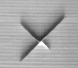
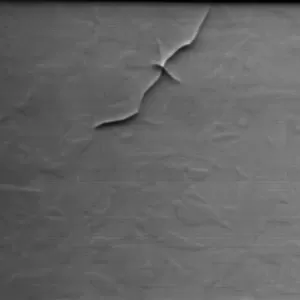
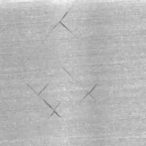
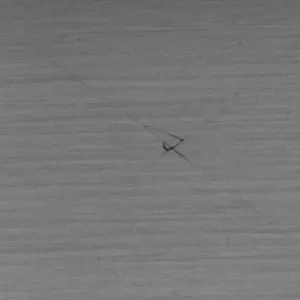
Crack Detection Equipment SC-MC-W is a high-precision automated inspection device specially developed by Vision Potential for defect detection of silicon wafers and cells in the photovoltaic industry. It innovatively integrates diverse inspection technologies such as TFC solution, TFC+visible light solution, TFC+backlight crack solution, bright-field backlight crack solution, dark-field backlight crack solution, combining NIR infrared imaging technology with AI intelligent algorithms to achieve full-cycle defect coverage from silicon material slicing to cell manufacturing processes. Multiple solutions can be switched on demand, adapting to multi-technology route cell products and different inspection scenarios, balancing production efficiency and inspection accuracy.
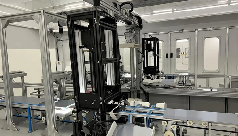
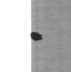
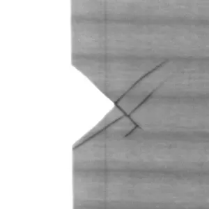
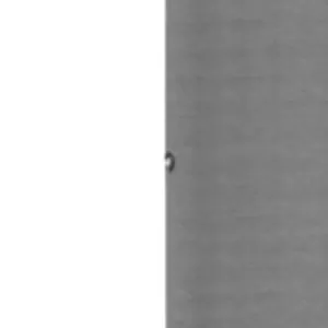
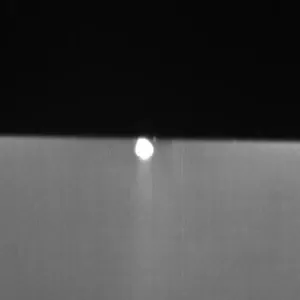
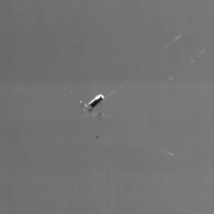
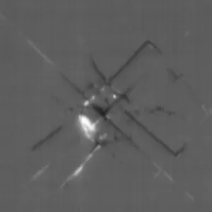
 SC-MC-W Device Diagram
Outgoing quality inspection and in-process inspection for mono/polycrystalline silicon wafers and quasi-mono slices after ingot cutting, accurately identifying defects such as cracks, broken pieces, silicon dropout, edge chipping, ensuring incoming material quality.
Incoming quality inspection for purchased silicon wafers and semi-finished cells, preventing unqualified materials from entering the production process and stabilizing production line operation.
Covers the entire process including texturing, diffusion, coating, etching, metallization, etc., adopting dark-field inspection solutions to effectively avoid issues like unclear imaging and interference common in traditional methods, real-time monitoring of process damage.
Supports customizable inspection parameters and flexible switching between multiple solutions, providing high-precision imaging data for research on PV material defect mechanisms and new algorithm validation.
Composed of four parts: camera module, light source module, machined structural parts, and computing module, ensuring stability and reliability.
Supports 156×156mm~210×210mm (half/full wafers) without changing adapter components.
Throughput ≥6000 pieces/hour, inspection time 0.25~0.5s, matching production line rhythm.
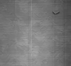
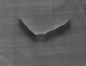
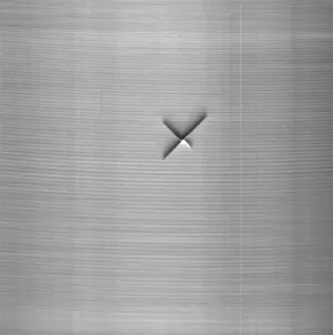
Accurate detection of typical defects such as cracks, edge chipping, corner breaks, fragments, silicon dropout.
One-click switching between bright-field/dark-field crack solutions and TFC series solutions, adapting to different materials/thicknesses.
Compatible with mainstream and emerging cell technologies such as PERC/TOPCon/HJT/xBC.
Online/offline machines seamlessly integrate with production lines, realizing fully automated inspection, sorting, and alarming processes.
AI algorithm automatically records defect location/type/size, generates inspection data for process traceability.
Imaging accuracy ≥0.1mm/pixel, multiple solutions capture minute defect details.
Core parameters such as exposure time, defect size/length/grayscale support manual customization.
Imaging data can be exported, compatible with third-party analysis software, meeting production statistics or academic research needs.
Multi-solution fast switching: one-click switch between bright-field/dark-field crack solutions and TFC series solutions, no extra debugging required
Solves the pain point of uneven imaging caused by diverse incoming material line directions in traditional equipment
Multi-technology route compatibility: PERC/TOPCon/HJT/xBC, poly/mono/quasi-mono wafers, and pre/post coating processes
Seamless full-process integration: dedicated solutions for incoming, texturing, coating, diffusion, etching, metallization, etc.
High-speed batch inspection: throughput ≥6000 pieces/hour, inspection time 0.25~0.5s
Full core defect coverage: cracks, edge chipping, corner breaks, fragments, silicon dropout, notches, scratches, no omission
Automated integration and traceability: seamless connection with production lines, AI automatically records defect location/type/size, generates inspection reports
Ultra-high imaging accuracy: 1k/4k resolution cameras, ≥0.1mm/pixel, 900~1700nm wavelength dedicated for crystalline silicon
Accurate defect detection: 50μm crack width recognition, effectively avoiding false detections caused by process fluctuations and surface contamination
Flexible hardware compatibility: full size coverage 156~210mm, custom stage, durable materials
Adjustable software parameters: manual customization of exposure time (10μs~1s), wavelength, focus distance (400-650mm)
Convenient data interaction: imaging data exportable, compatible with third-party software, standard Windows AI inspection software
| Parameter | Specification |
|---|---|
| Model | SC-MC-W |
| Camera Specifications | NIR enhanced InGaAs camera / 4K line scan CMOS, 1k/4k pixels, exposure 10μs~10s, response 900-1700nm |
| Infrared Pixels | 1024*1 pixels / 4096*2 pixels |
| Lens Specifications | HD wide-angle 16/25/45mm optional, FOV ≥80°, telephoto lens optional |
| Light Source Specifications | Semiconductor laser, wavelength 1100±5nm / 1300±5nm / 1450±5nm |
| Spot Uniformity | ≥90% (within effective detection area) |
| Exposure Cycle | 20μs~10000μs, step 1ms adjustable |
| Detection Wavelength Range | 900~1700nm (for crystalline silicon) |
| Compatible Sizes | 156×156mm ~ 210×210mm (half/full wafers) |
| Wafer Thickness | 160~200μm |
| Inspection Objects | Crystalline silicon cells (PERC/TOPCon/HJT/xBC); pre-coating / pre-process cells |
| Detectable Defect Types | Cracks, edge chipping, silicon dropout, notches, corner breaks, fragments, scratches, etc. |
| Stage Size | Adaptable to automated tracks (customizable) |
| Control Method | Proprietary host software fully automated control |
| Detection Accuracy | Crack width > 50μm detectable |
| Imaging Accuracy | ≥0.1mm/pixel |
| Focus Mode / Distance | Manual focus / 400-650mm |
| Hardware Mount | Aluminum profile, sheet metal, etc. |
| Inspection Time | 0.25s~2s (based on automation cycle) |
| Test Platform | Windows + standard AI inspection software |
| Power | 500-1000W |
| Power Supply Protection | Reverse current/overload/leakage/ESD/overheat protection |
| Computing Device | Industrial computer |
| Ambient Temperature | 15-50℃, Humidity 30%-70% (non-condensing) |
| Equipment Weight | Approx. 20kg (actual product prevails) |
| Dimensions | 350×250×600mm (L×W×H) |
| Power Supply | Single-phase AC220V±10%, 50HZ±1HZ |
A high-precision automated inspection device specially developed for defect detection of silicon wafers and cells in the photovoltaic industry. It innovatively integrates diverse inspection technologies such as TFC solution, TFC+visible light solution, TFC+backlight crack solution, bright-field backlight crack solution, dark-field backlight crack solution, combining NIR infrared imaging technology with AI intelligent algorithms to achieve full-cycle defect coverage from silicon material slicing to cell manufacturing processes. Multiple solutions can be switched on demand, adapting to multi-technology route cell products and different inspection scenarios, balancing production efficiency and inspection accuracy, providing users with flexible and efficient customized inspection solutions.
contact
Be the first to know about our new product launches, latest blog posts and more. Nanjing Vision Potential Intelligent Technology Co.,Ltd.Established based on the Nanjing Xiangning Artificial Intelligence Research Institute, we have brought together a number of outstanding industry... Any question or request?
Click below, we’ll be happy to assist. contact